Miniaturization of IC Packages
An overview of QFP, QFP, BGA and WLSCP packages.
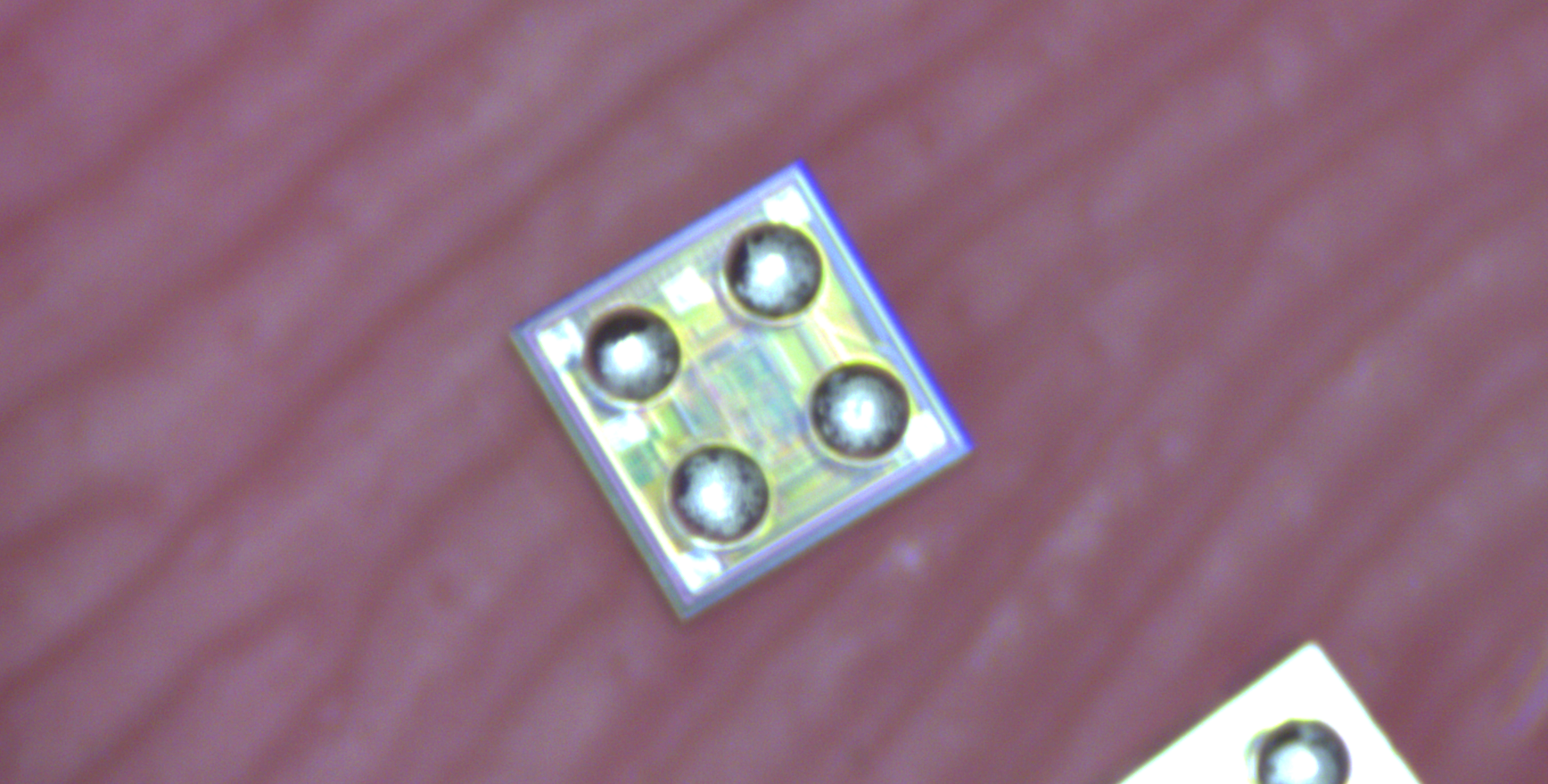 A 0.5 mm pitch BGA microscope image on a finger tip.
Multipart Series
Part 2: Exploring IC Package Miniaturization: QFP and QFN
Part 3: The move from QFN and QFP to Ball Grid Array
Part 4: The Rise of Wafer Level Chip Scale Packages (WLCSP)
Part 5: All the IC Package Data in One Place: QFP, QFN, BGA, and WLCSP
In the ever-evolving landscape of electronics, the drive towards miniaturization and efficiency has led to significant advancements in packaging technologies. Two of the most notable packaging methods that have adapted to this trend are Ball Grid Array (BGA) and Wafer-Level Chip Scale Packaging (WLCSP). Both technologies are replacing traditional packaging methods such as the Quad Flat Package (QFP) and Quad Flat No-lead Package (QFN) for ICs.
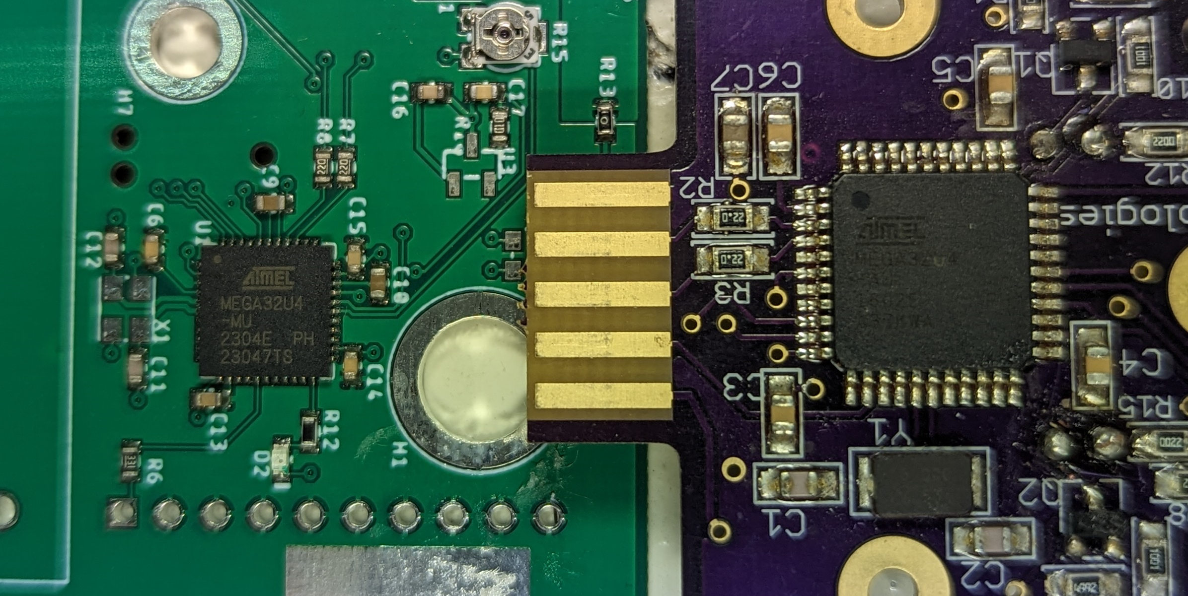 An ATMega32u4 microcontroller in a 44-QFN package on the left and a 44-QFP package on the right.
Quad Flat Package (QFP)
QFPs are characterized by having "gull-wing" leads extending from all four sides of the rectangular package. These leads are soldered to the PCB, with all of the solder joints visible well outside of the package. QFPs can accommodate a large number of pins, ranging from 20 to 304, making them suitable for integrated circuits that require many connections, such as microprocessors and microcontrollers. The pitch on QFP packages varies from 0.8 mm down to 0.4 mm, with the number of leads ranging from 32 to 256.
Quad Flat No-lead Package (QFN)
QFNs are similar in shape to QFPs but do not have leads. Instead, electrical connections are made through pads at the bottom of the package, which are designed to be soldered directly to the PCB. The absence of leads allows QFNs to have a smaller footprint and lower profile compared to QFPs. QFNs also typically include a thermal pad at the bottom to enhance thermal performance. The pitch on QFN packages varies from 0.8 mm down to 0.4 mm, with the number of leads ranging from 12 to 80.
Ball Grid Array (BGA) Packaging
The BGA's footprint, characterized by an array of solder balls on the package's underside, allows for a more efficient use of space on the PCB compared to traditional leaded packages. As devices have become more complex and the demand for smaller electronic products has increased, BGA packaging technology has evolved. Manufacturers are now producing BGAs with smaller solder balls and tighter pitches, enabling a greater number of I/O connections in a smaller area. This miniaturization trend has facilitated the development of compact, high-performance devices such as smartphones, tablets, and wearable technology. Pitches vary from 1.0 mm down to 0.4 mm, and even 0.35 mm for some chips with a lower ball count, with the number of balls ranging from as low as 4 to over 500.
Wafer-Level Chip Scale Packaging (WLCSP)
Wafer-Level Chip Scale Packaging (WLCSP) represents a significant advancement in semiconductor packaging technology, where the packaging process occurs simultaneously with wafer fabrication. This approach ensures that the final package size is virtually the same as the silicon die itself, dramatically reducing the overall footprint of the packaged device. WLCSP enables more efficient use of space on printed circuit boards, improving thermal and electrical performance due to shorter interconnect distances. Additionally, by integrating the packaging process into wafer fabrication, WLCSP offers cost advantages over traditional packaging methods. It is particularly favored for the production of compact, high-density devices such as smartphones, wearables, and medical devices, where space efficiency and performance are paramount. WLCSP packages typically have pitches of 0.5 mm, 0.4 mm, 0.35 mm or 0.3 mm, with ball counts starting at 4 for the smallest packages to over 200.
Trends Toward Miniaturization
The trend toward miniaturization in BGA and WLP footprints is driven by several factors, including the demand for portable, lightweight devices, the need for faster data processing and communication, and the desire for lower power consumption. To meet these requirements, packaging technologies are continually being refined.
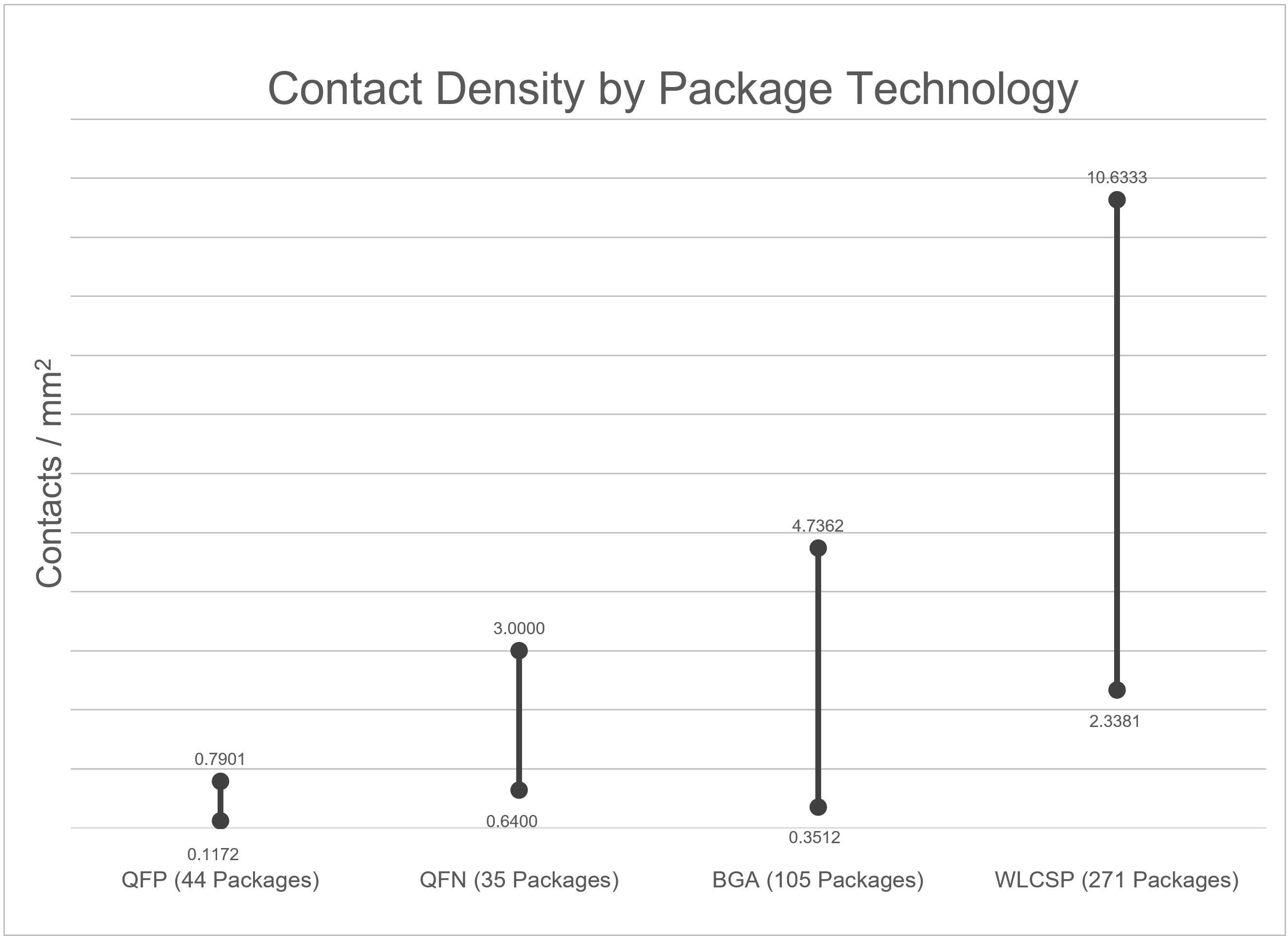
This trend is evident when looking at the contact densities for each of these progressively miniaturized packages. A dataset for more than 400 QFP, QFN, BGA, or WLCSP packages was collected, and the contact density was calculated as the number of balls per square mm or the number of leads per square mm.
Get More information
Part 2: Exploring IC Package Miniaturization: QFP and QFN
Part 3: The move from QFN and QFP to Ball Grid Array
Part 4: The Rise of Wafer Level Chip Scale Packages (WLCSP)
Part 5: All the IC Package Data in One Place: QFP, QFN, BGA, and WLCSP
For more information sign up at here. If you have any questions small components on your PCB reachout to us here.