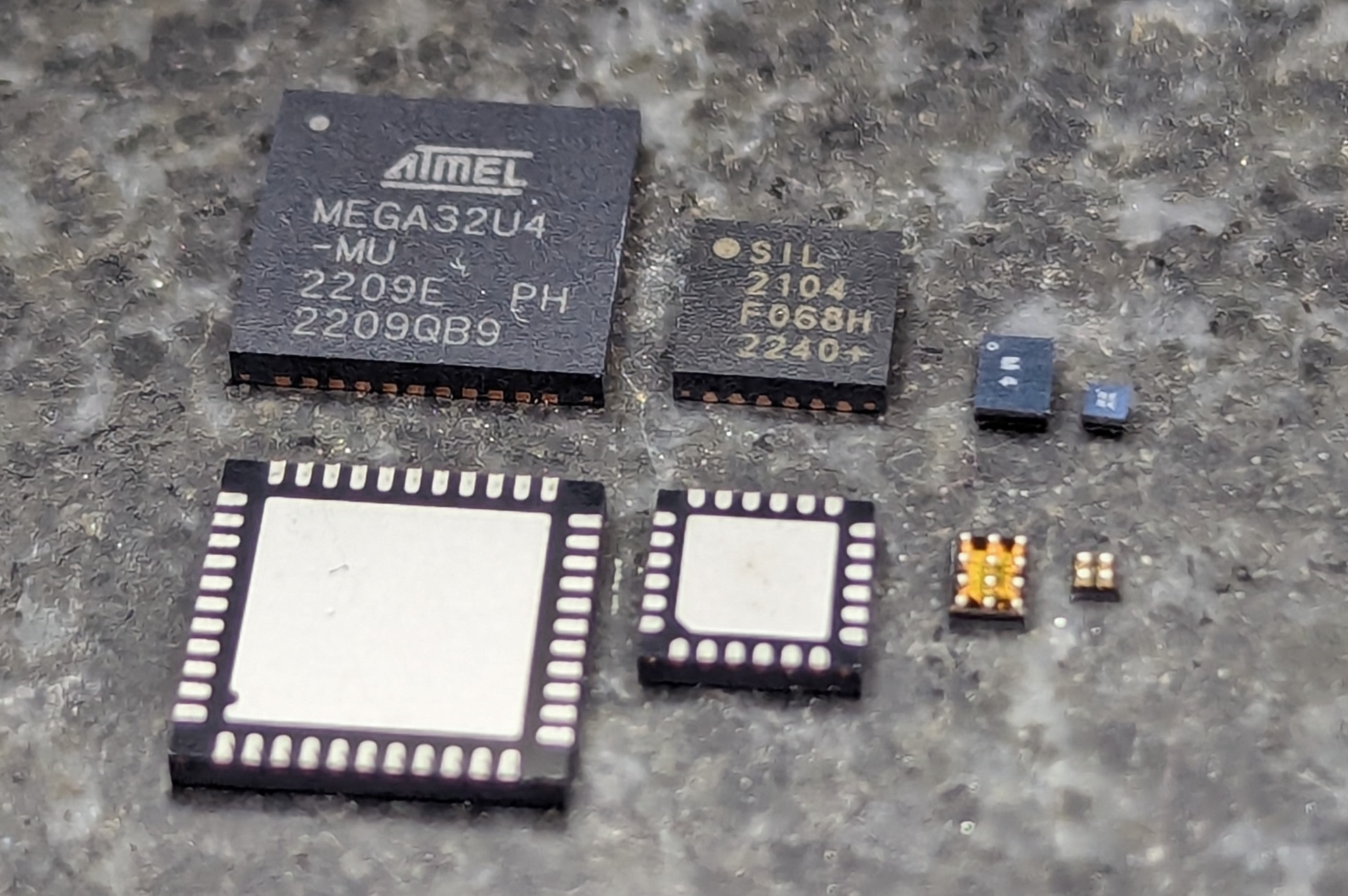
The move from QFN and QFP to Ball Grid Array
A deeper look at the move Quad Flat Packages and Quad Flat No Lead to Ball Grid Array packages
This is the third blog post in our series about the miniaturization of IC packages. To see a overview of the four types of package we will look at in the this series visit the first post and for a deeper look at package density for Quad Flat Packages (QFP) and Quad Flat No Lead (QFN) see our second post. In our fourth post we have an indepth look at WLCSP. In our fifth post we share all the data we collected in this blog series.
Why move to BGA
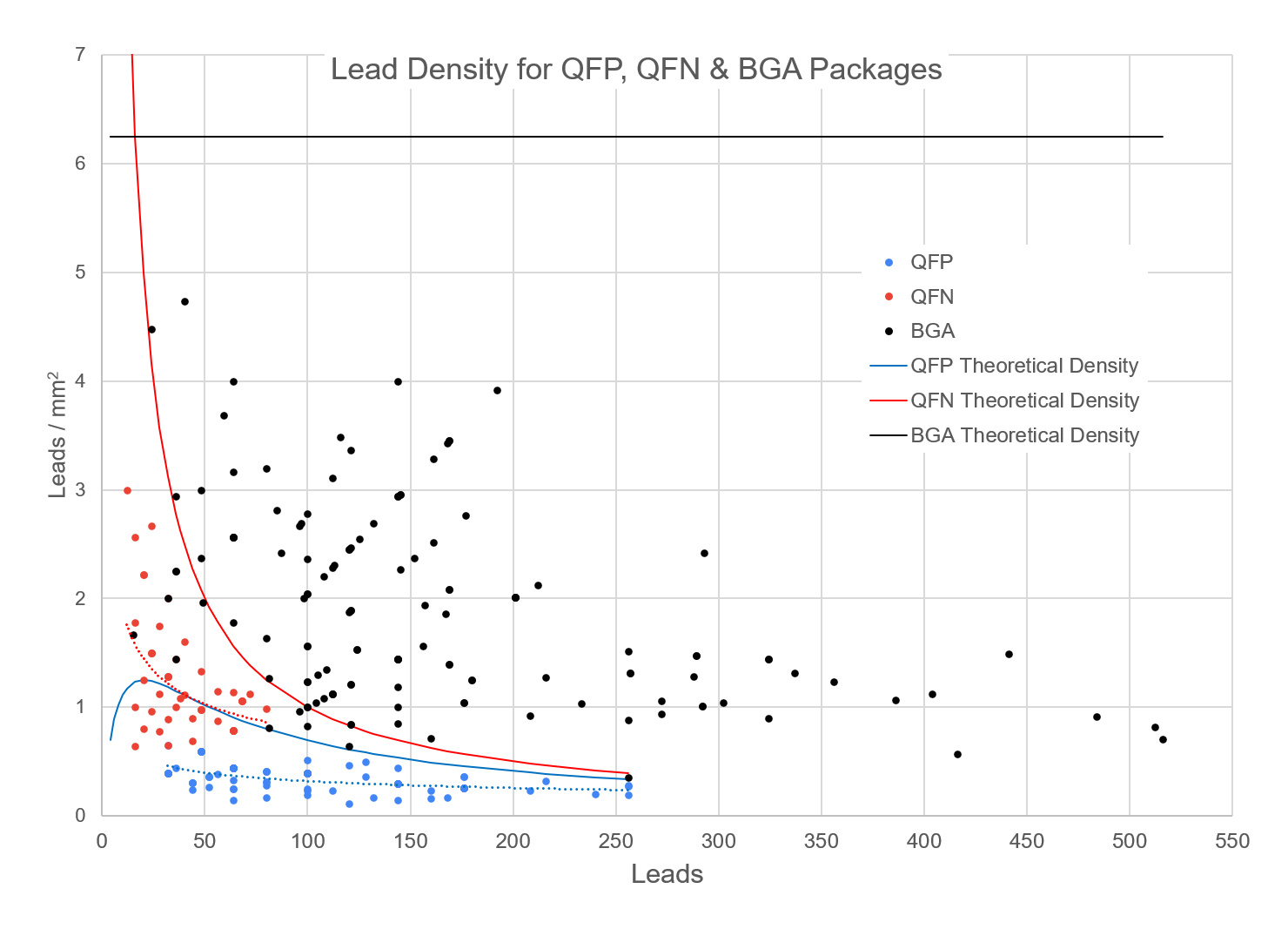
The shift from QFPs and QFNs to Ball Grid Array (BGA) packages primarily occurred due to the need for smaller, more compact, and higher-performance electronic devices. As we saw in our analysis of pin density for QFPs and QFNs as chips require more contacts their space efficiency has diminishing returns. Ball Grid Array chips solve this by utilizing the entire aera under the chip.
BGAs have several other advantages particularly over QFPs without a thermal pad that many QFNs have. BGA packages typically have shorter electrical paths between the integrated circuit and the package's pins, leading to improved electrical performance, such as reduced signal delays and better high-frequency characteristics. The solder balls used in BGA packages provide better thermal conductivity compared to the leads of QFPs. This allows for more efficient heat dissipation, which is crucial for high-performance electronic devices, such as CPUs and GPUs. BGA packages offer better mechanical robustness than QFPs because the solder balls distribute the mechanical stresses more evenly across the package. This reduces the risk of damage from mechanical shocks and vibrations, making BGA packages suitable for portable and rugged applications.
Package Data
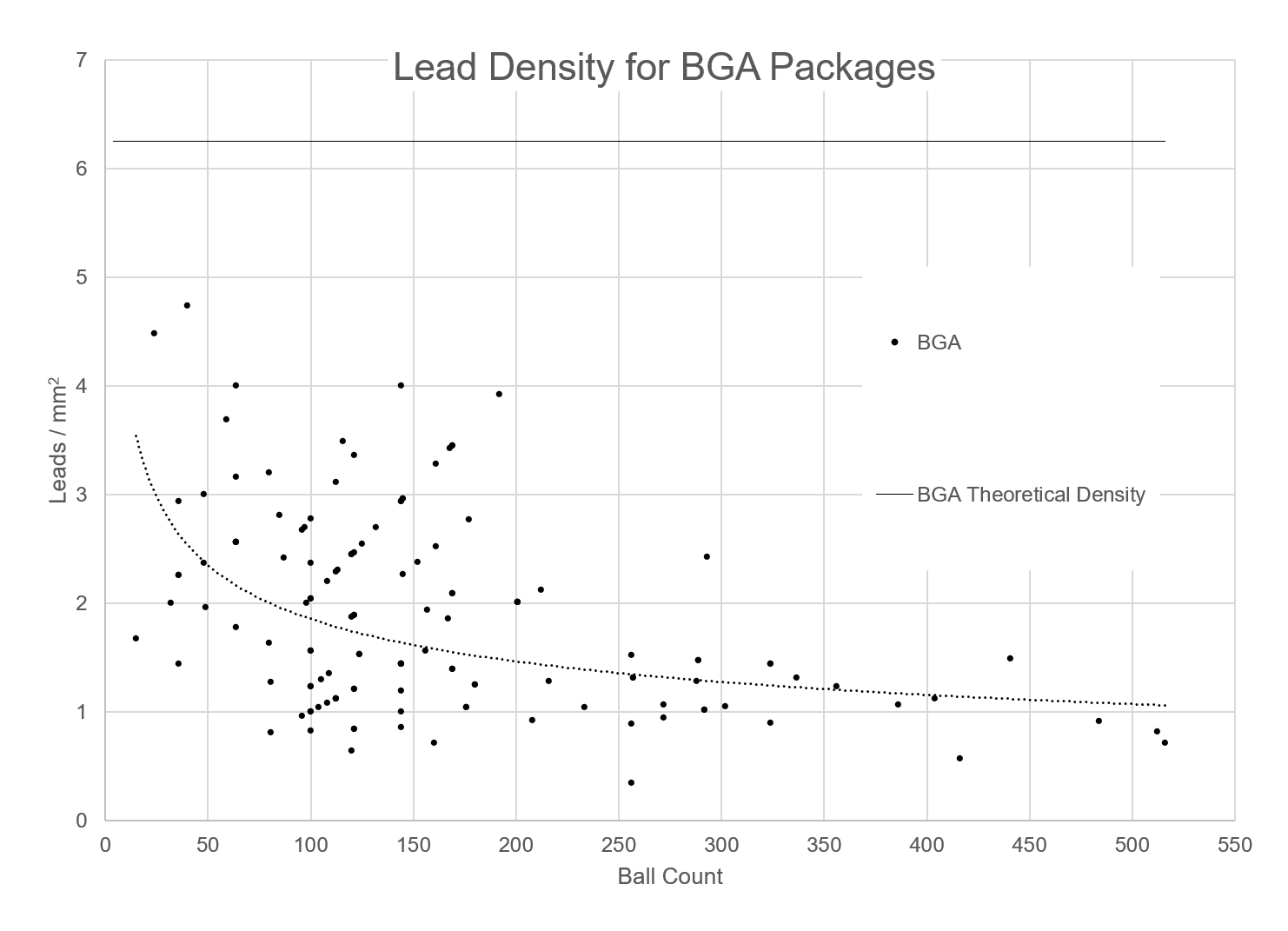
We compiled data on 105 different, unique BGA packages for this analysis. These packages were identified through queries of Digi-Key’s inventory of in-stock components.
The pitch varies from 1mm to 0.4mm, with the higher lead count packages generally having larger pitches, unlike QFNs and QFPs from earlier blog posts.
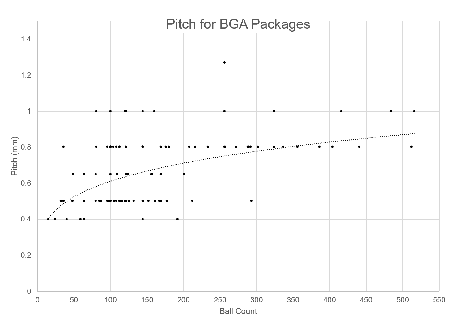
The larger pitches in the higher ball count BGAs increase the yield rate for good solder joints, counteracting the decrease due to the large ball count. The increase in yield for the large pitch components comes from the larger balls, thus allowing a larger ball solder paste, like a T3, to be used, which makes the wetting of the solder easier. The larger pitch and larger ball also result in a larger opening in the solder stencil, eliminating defects with solder paste application, such as misalignment, partial prints, scooping, and peaking. The larger pitches also eliminate the risk of solder bridging between the balls of the BGA.
Max Theoretical Lead Density
The max theoretical lead density for a BGA is derived from the pitch. The typical minimum pitch before getting int wafer level packaging is 0.4mm. We can calculate the lead density by looking at the aera each ball occupies:
BGA Inspection
A significant difference between the BGA and Quad packages is the ability to inspect the solder joints. For QFNs and QFPs, it's easy to visually inspect each joint. However, BGAs have joints hidden under the components, not directly visible with typical visual inspection techniques. There are generally a couple of methods for inspecting BGA solder joints: the destructive testing method is a pry test, and the non-destructive tests are side view visual inspection and x-ray inspection.
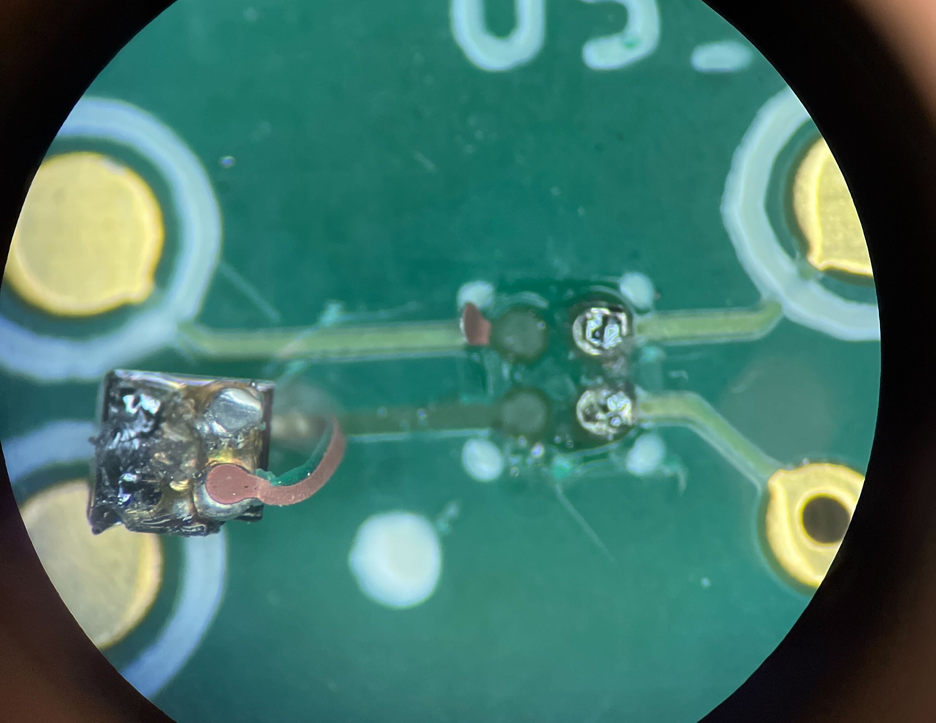
We use the destructive pry tests to develop our solder reflow profiles and select solder pastes as we improve our capabilities. This test involves reflowing the joints and then prying them off the PCB. With good solder joints, this can result in tearing pads and possibly traces off the PCB with the component. A bad joint will show smooth, wetted joints on either the PCB side or component side. We will also occasionally dye the joints before prying the component off, to accentuate the good joints.
The side view visual inspection involves using an inspection system to visually look between the rows of solder balls. This method allows all of the balls to be visually inspected and can easily detect solder bridges between the balls and determine good wetting of the component side and PCB side pads. However, this method does require room around all the BGA and is time-consuming, as each row needs to be inspected separately.
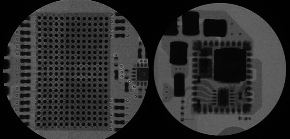
X-ray inspection is our preferred method of inspection, as it allows us to easily inspect each ball's solder joint all at once, plus see voids in any solder joint on the PCB. This method is useful for more than just BGAs; many QFN packages contain a larger thermal pad on the bottom. The x-ray inspection tools allow us to see voids in the large joints. We have recently purchased an x-ray inspection machine to allow us to inspect larger arrays of BGAs and larger solder joints on our PCBs.
Get More Information
Part 1: Miniaturization of IC Packages
Part 2: Exploring IC Package Miniaturization: QFP and QFN
Part 4: The Rise of Wafer Level Chip Scale Packages (WLCSP)
Part 5: All the IC Package Data in One Place: QFP, QFN, BGA, and WLCSP
For more information sign up at here.