What is FlashPCB's stackup?
Checkout our standard 2 and 4 layer stackups
The PCB stackup is a drawing of the cross section of the PCB itself showing the layer weights and construction of the board. The most important layers shown on the stack up are the copper layers the dielectric layers between the copper layers and the substrate itself. most PCB designers think of the PCB should be layers in terms of a 2D problem when we go to manufacture we have to make it physical 3D good and this is where the stack up becomes important. Simple two and four layer boards will use a very standard stack up some as the layer count increases the stack up begins to vary significantly.
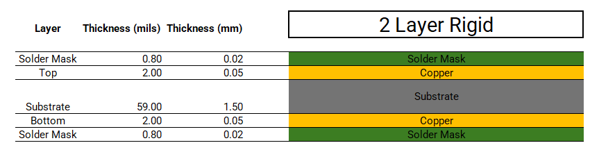
2 Layer Stackup
At flash PCB we offer two different stack ups one for our two layer board and one for our four layer board. Both of these boards are 1.6mm thick and both have 1oz copper on the outside layers. For more information about copper weight see our Basics of PCB Layers blog post.
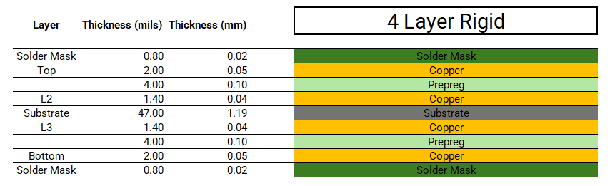
4 Layer Stackup
While our standard four layer stackup has 0.5 oz copper on the inner layers.
Custom Stackup
If you need a custom stackup for your PCB project please feel free to e-mail us at quote@flashpcb.com.