The Basics of PCB Layers
What are the layers and what do they do?
PCBs, or printed circuit boards, are present in almost every electronic device from computers, cell phones, cars, medical devices to fridges, toasters and light bulbs. Single-layer PCBs were the first used, but today multi-layer PCBs allow for increased functionality and miniaturization of electronic devices.
Layer Demo
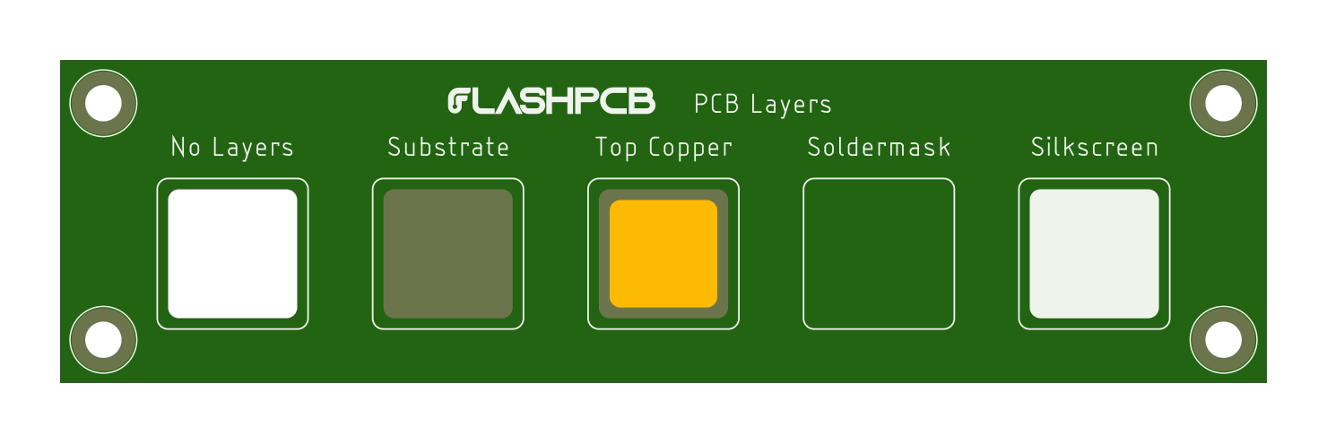
We have created a PCB that shows each layer. From left to right we have: no layers, just substrate, just copper on the substrate, copper with soldermask and finally soldermask with silkscreen on top. Below is the Eagle project for this board.
Substrate
PCBs are made up of multiple layers adhered to a substrate. There are a variety of materials that can be used as the substrate for a PCB, including fiberglass (FR-4), Aluminum, Ceramics (Rogers) and flexible PTFE or Polyimide. The most common substrate material is fiberglass referred to as “FR-4”. Fiberglass is a popular choice due to its thermal stability, mechanical strength, mechanical toughness, and high thermal resistance. Aluminum substrates are more common in high-power applications as they have good thermal conductivity and transfer heat away from hot components like LEDs.
Most PCBs are rigid, however, there are some applications requiring flexible circuits. In these cases flexible PTFE or Polyimide substrates are used. These are typically seen in tightly packaged devices where multiple electrical connections need to be made between boards. Special consideration needs to be paid to the design of flexible PCBS.
Copper
The next layer is the copper layer, which is where the actual circuits are printed. This layer is made up of thin copper foil that is laminated onto the substrate. The copper is etched in a specific pattern to create the circuit pathways that will connect the various components of the device.
The thickness of the copper foil is usually measured in ounces, which refers to the number of ounces of copper in one square foot. A typical board will have 1oz on the top and bottom layers of cooper and 1oz or 0.5oz on the inner layers of copper.
Solder mask
On top of the copper layer is the solder mask. Solder mask is what gives the PCB its distinctive green color. The solder mask helps to prevent short circuits by providing an insulator over the copper layers, only exposing the areas that need to be soldered. The solder mask layer also helps in the manufacturing process by forming “solder mask dams” between fine pitch pads preventing bridges between leads of the components.
Solder mask is typically green, although other colors like black, red, blue, white and purple are available today. The green color is most common because it aids inspections, allows for the smallest solder mask dams of all the colors and is typically cheaper due to its frequent usage. FlashPCB currently only offers green but will add support for black PCBs soon.
Silkscreen
The next layer is the silkscreen, which is a layer of ink that is used to print labels and other identifying information onto the PCB. This can include the names of the various components and their locations on the PCB. The silkscreen can only be printed on top of the solder mask.
White and black are the most common colors of silk screen printing. Currently FlashPCB only offers white silkscreen printing.
Layer count
The number of layers in a PCB refers to the number of copper layers in the board. Today two and four layer layer boards are most typically used, very complex PCBs like computer motherboards may have up to 32 layers. We have even seen a 180 layer board at a trade show (it was half an inch thick). In very high layer counts like this, many of the layers are dedicated to ground and power planes. Typically in a four layer board, the inner layers are ground and power planes while signal traces are run on the top and bottom layers.
It's worth noting that PCBs with a higher layer count are generally more expensive to manufacture due to the additional material and fabrication process required. However, the additional cost can be offset by the improved performance and functionality that is possible with a multi-layer PCB. FlashPCB currently supports two and four layer boards.