Adding Power Planes to KiCad Boards
Why and how to use KiCad's "Filled Zone" tool
Power planes, copper pours, or filled zones, in KiCad terminology, are often used to route power and ground connections by filling the entire area between traces with copper. We will discuss why you want to do this on your board and how to add the zones in KiCad. We will also discuss considerations for manufacturability.
Why add power planes
Power planes increase the current carrying capacity of your power signals. On a PCB, the current carrying capacity of a trace is determined by its width and so for high current connections we typically want a wider trace. Power planes are essentially the widest trace we can achieve on a particular board.
Power planes reduce electrical noise on PCBs by shortening the return path to ground and decoupling the individual circuits on the board. A good ground plane provides a direct return path for every component on the board to ground rail location on the board. This eliminates any chance of ground loops or poor ground connections for the circuits on the PCB. Using power planes also decouples the individual circuits on the board. Voltage transients in a noisy circuit are passed down the individual trace to the next circuit whereas in a power plane they're dissipated across the plane.
Power plants also provide a good way to dissipate heat on a PCB. Copper, known to us as a good conductor of electricity, is also a good conductor of heat, and the amount of heat it can conduct away is proportional to its area. On many packages there is an exposed pad that acts as both a thermal pad and a ground connection. It’s most effective when it’s connected to a large ground plane to help dissipate the heat from the package. If that thermal pad was connected to a thin ground trace it wouldn't have the same heat dissipation capacity.
Power planes make it much easier and cleaner to route a PCB. This is particularly the case on four layer boards in which often the second layer is a ground plane and the third layer is a power plane, leaving the top layer of the board for all the high frequency traces and the bottom layer of the board for other less sensitive traces.
Design consideration for filled zones in KiCad
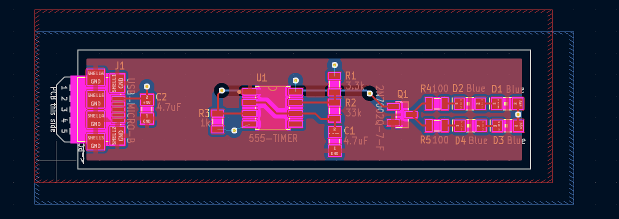
KiCad by default will fill the zones up to the edge of the PCB. This can often lead to shorts between the different layers of copper. These shorts are caused by copper chips in the milling or scoring operations at the edge of the PCB. You can change the distance to the edge of the board by going to File > Board Setup > Design Rules > Constraints and adjusting “Copper to edge clearance”. We recommend 1.0 mm.
Part of a filled zone may become disconnected from the rest, resulting in a floating plane. This can resonate and emit EMI energy. This problem is more often seen on two-layer boards. One way to solve this is by stitching the zones together with vias.
Most components will need thermal breaks if they are directly connected to a filled zone. When filling zones in KiCad you might notice most component pads are only connected by four smaller traces. This is designed to reduce the need to heat a large copper plane to solder the components while only introducing a small amount of impedance in the connection to the filled zone. During reflow, a pad without a thermal break will take longer to reach the solder reflow temperature and this may lead to tombstoning or misaligned components. Well-designed libraries like the FlashPCB library already account for thermal breaks.
How to add filled zones in KiCad
- Select which net will be placed on which layer. For two layer boards I typically look for the net with the most connections for the top layer, but this selection may be defined by the need to place a ground plane to dissipate heat on the other side of your components with thermal paths. On a four layer board the second layer is typically a ground pane and the third layer is typically a power plane.
- Click the add filled zone tool.
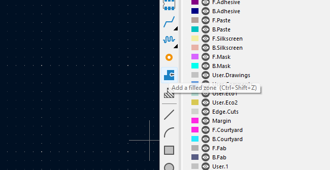
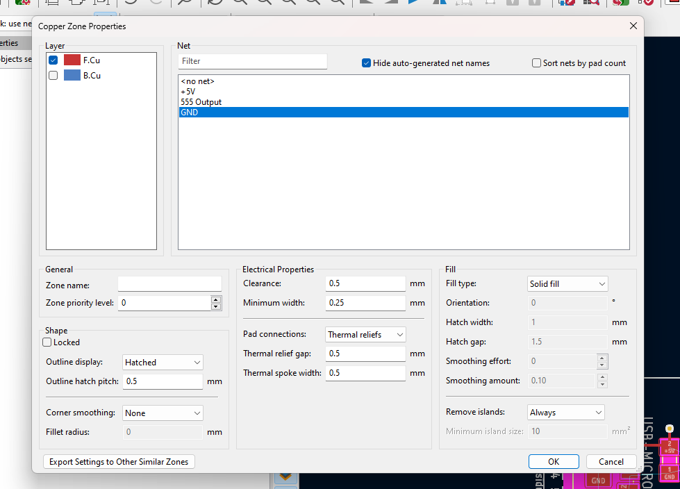
- Select the appropriate copper layer and net in the Copper Zone Properties.
- Draw a the zone around the entire board.
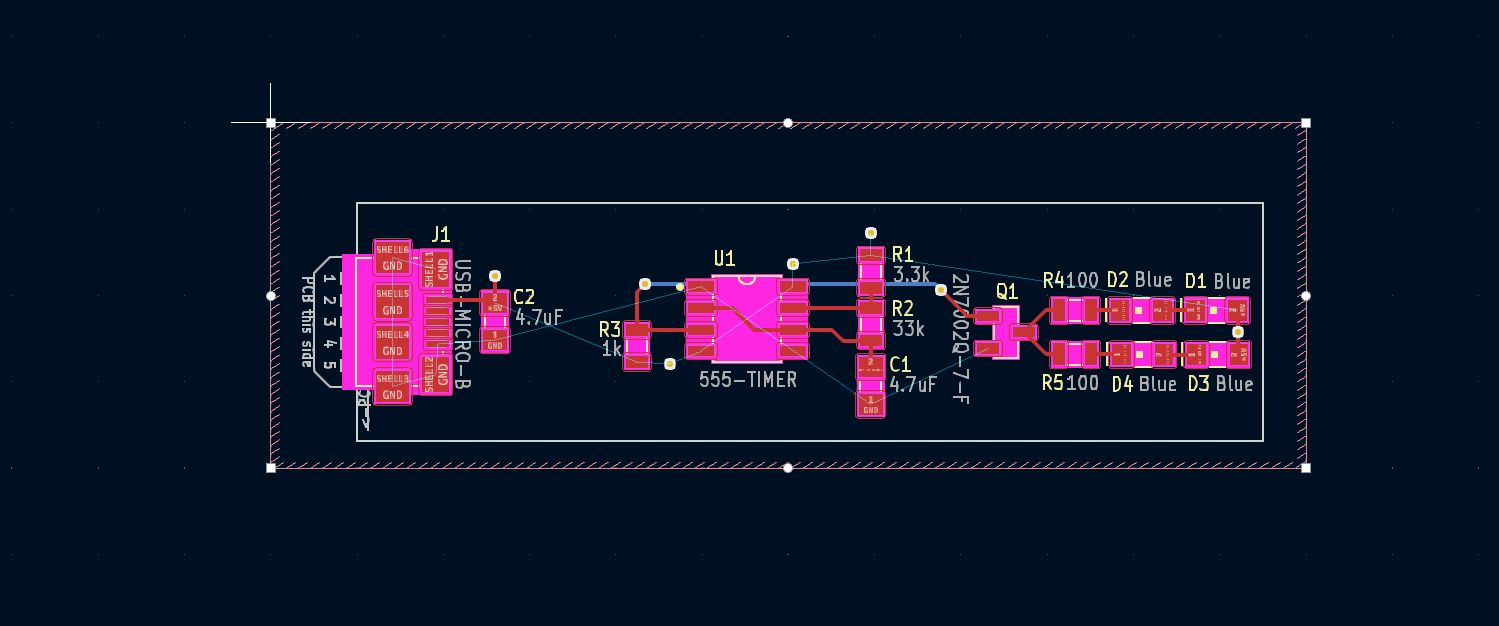
- Repeat for each desired plane.

- Adjust “Copper to edge clearance” in File > Board Setup > Design Rules > Constraints.

- Press “b” to refill zones.
Get information about upcoming features
For more information sign up at here.