Designing Plated and Non-plated Slots in EAGLE
How to ensure your design intent for plated and non-plated slots is well defined
Overview
As Surface Mount connectors become smaller and more compact it is essential to understand how to properly design board features to support fine pitch pad arrays. Such features are becoming the norm for current and next generation connectors such as USB-C, MicroSD, and others. Many of these connectors employ a combination of plated through holes (PTH) and non-plated through holes (NPTH) to ensure the connector remains in place during the assembly process and has adequate mechanical connection to the board to ensure reliability over the lifetime of the design. This blog will cover some best practices for creating PTHs and NPTHs in AutoDesk EAGLE, and provide a deeper understanding of how these features are manufactured.
Using Autodesk EAGLE
While AutoDesk EAGLE is one of the most popular CAD softwares due to its accessibility and longevity, it unfortunately falls short when it comes to designing plated or non-plated slots that are not simple round holes. For this reason it is recommended to use KiCad for designs that heavily incorporate USB-C, HDMI, MicroSD, or other fine pitch connectors which require PTHs or NPTHs. This is not to say that designing such features are impossible in EAGLE, however they require significantly more effort in order to be properly employed with minimal room for misinterpretation by the PCB panel fabricator. Making these features in KiCad will be covered in a separate blog as it is also an involved process.
Mechanical fabrication process overview
Before we get into the process of creating these features in CAD, let’s discuss the manufacturing process required for creating slots on a PCB. Slots on a PCB are typically created by either drilling a series of holes using a mechanical drill, or by using a mechanical end mill router or laser cutter to remove material from the PCB panel in the specified shape. Plated slots follow a very similar manufacturing process to vias or THT pads wherein the copper pads are created on the board during the plating process and then material is cut out at a later point in the manufacturing process; once the materials are removed to create the desired slot shape a special plating process is used to apply copper, gold, or other specified material finish to the inside of the cut to connect the top and bottom layers. Non-plated slots are instead simply drilled or milled to the desired shape as there is no copper plating around or inside the hole. Use of non-plated holes and slots have become a very popular method for fine pitch components to remain secured during the placement and reflow processes to ensure that the connectors do not shift and cause bridged connections or poor quality solder joints. Plated slots are very useful for relieving mechanical stress from the connecting pads, and therefore can be found on many connectors, switches, trimmer-potentiometers, or other mount points which are designed to experience mechanical stress during use.
Required EAGLE Layers
Creating Plated or Unplated Slots in Eagle is a detailed process with important steps that cannot be overlooked. We will cover the necessary steps below. The layers used to create these features are Copper Layers Top through Bottom (1-16), Pads (17), tStop(29) and bStop(30), tKeepout(39) and bKeepout(40), and Milling(47). For holes and non-plated slots layer Dimension(20) may possibly be used in place of Milling(47) but this is not recommended.
Step-by-Step Instructions
Step 1: Layer 47 (Milling)
Draw the desired slot shape as a wire/line using the Milling layer (Layer 47). This step will be the same for both plated and non-plated slots; please note that inner corners (angle under 180*) of a slot must be rounded with curve diameter >= 0.2mm in order to be manufacturable.
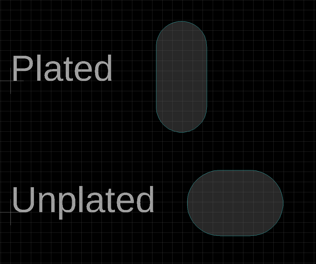 Figure 1: Light Blue Solid line is Milling (47)
Step 2: Layers 1-16 (Copper)
Please note that this step contains slightly different instructions to support a plated versus non-plated slot, this is integral to ensure the PCB panel fabrication software understands the design intent.
Making Copper Layer Polygons
Create a Top (Layer 1) or Bottom (Layer 16) polygon around the milling area which extends approximately +/- 0.2mm around the milling shape. This polygon must be copied and re-used for all relevant copper layers (typically Layers 1 through 16 including those in between for non-plated slots).
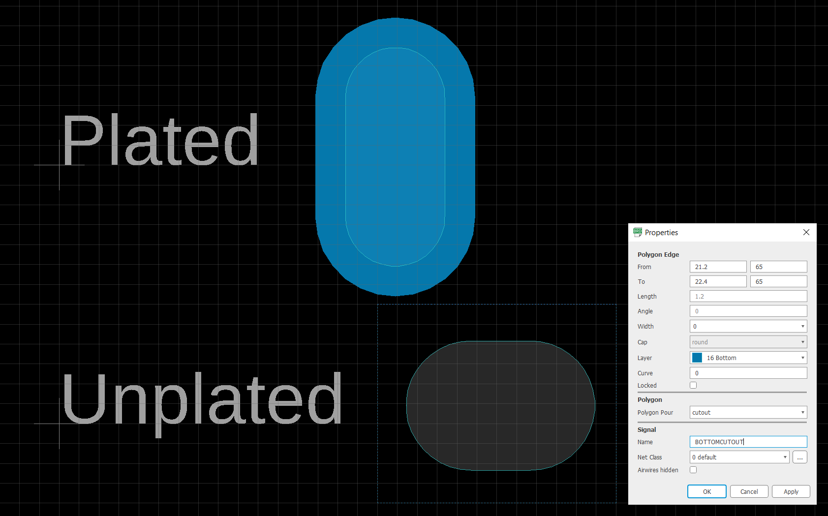 Figure 2: Copper Polygons pour type fill vs cutout
Once the Top layer polygon has been created, copy and paste the polygon making sure to re-assign each copy to the relevant copper layers. For plated slots, this would typically be Top and Bottom only, but for non-plated slots this would be all copper layers used in your design meaning Top, Route2, Route15, and Bottom for a 4 layer circuit.
NOTE for Non-plated Slots
IMPORTANT: for non-plated slots the copper polygons MUST have the “Polygon Pour” property set to “cutout”. This will ensure that any copper from a plane which intersects the milling shape is removed; if the cutout polygons are not added there is the possibility the PCB fabricator does not understand the design intent, and may not create the milled slot as designed.
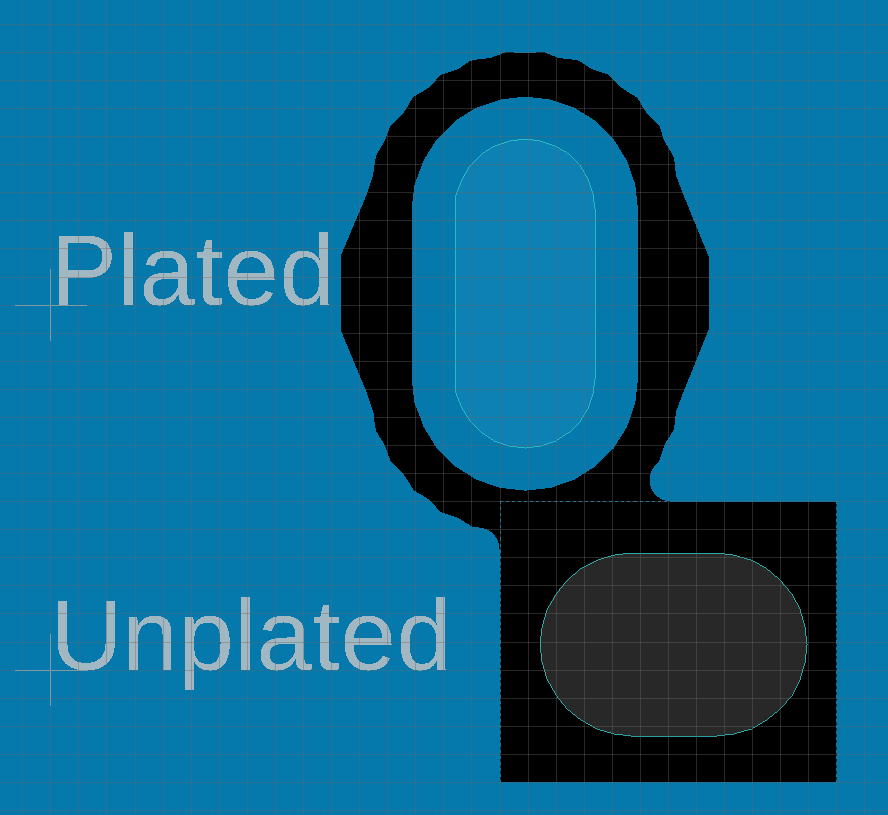 Figure 3: Copper polygons show where copper(blue) will be when 'ratsnest' is ran
Step 3: Layers 29,30 (tStop, bStop)
Now that the copper polygons and milling cuts have been defined, the next step is to define the tStop/bStop layers in order to determine where the Soldermask layer will not be applied. This step is critical for plated slots to ensure the top and bottom copper is exposed for soldering. For unplated slots this step is not as important but is still good practice to remove any possibility of misinterpretation during panel fabrication.
Making tStop/bStop Polygons
To create the tStop/bStop features, simply copy the copper polygons from 2B and paste them as tStop and bStop. For plated slots it is recommended to increase the size of the polygon by 0.1mm or more in all directions so that there will be a buffer zone between where the solder mask ends and copper plating begins.
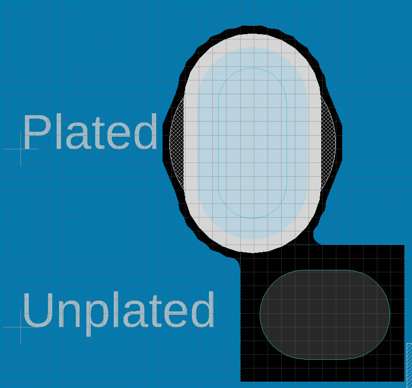 Figure 4: White area represents tStop/bStop which are ‘negatives', meaning that solder mask will be applied everywhere that tStop/bStop are not present
Step 4: Pads to Indicate Plating
This step is only applicable to plated slots. In order to indicate that a milled slot must have plating applied to the inside of the milled area, it is necessary to add a Through Hole Pad (layer 17) over the milling shape from 2A. The pad should contain a drill size equivalent to the width of the Milling shape, and the annular ring around the pad should be at least as large as the copper polygon around the Milling shape. In addition to indicating that this Milled slot must be plated, the Through Hole Pad also prevents copper planes from intersecting with the Top, Bottom, and Inner copper around the milled slot.
 Figure 5: Through Hole Pad over Milling operation to indicate Milled shape should be plated and inner copper from other planes must be removed
Step 5: Layers 39,40 (tKeepout, bKeepout)
The final step for creating the milled slots is to add tKeepout(39) and bKeepout(40) layers. These layers will ensure that no other components are accidentally placed to occupy the same location as these slots. It is recommended to add a buffer area of 0.1mm or larger based upon the tolerance stated on the component’s datasheet. Typically bKeepout should only cover the pins/posts which poke through to the bottom side of the board for soldering.
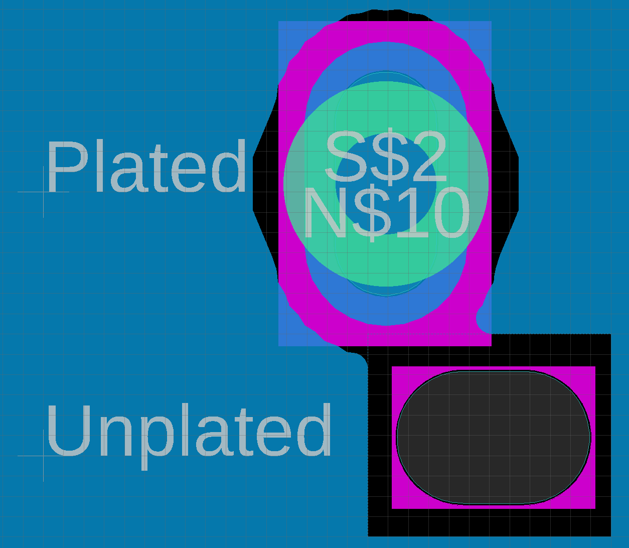 Figure 6: bKeepout (pink) is shows space reserved to be occupied by pins/posts, it is not necessary to keep inside the milling clear of bKeepout layer as we have done here
Final Result!
Done! There should be no color under the non-plated milling operation after running ‘ratsnest’ if the copper polygons were set to “cutout” pour type. Below is an image of the manufactured PCB created from this design.
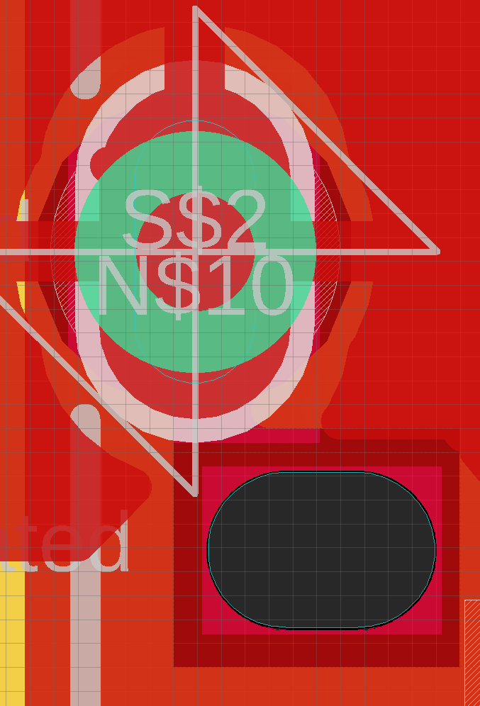 Figure 7: Final design in use with ratsnest showing the many different layers
Manufactured Product
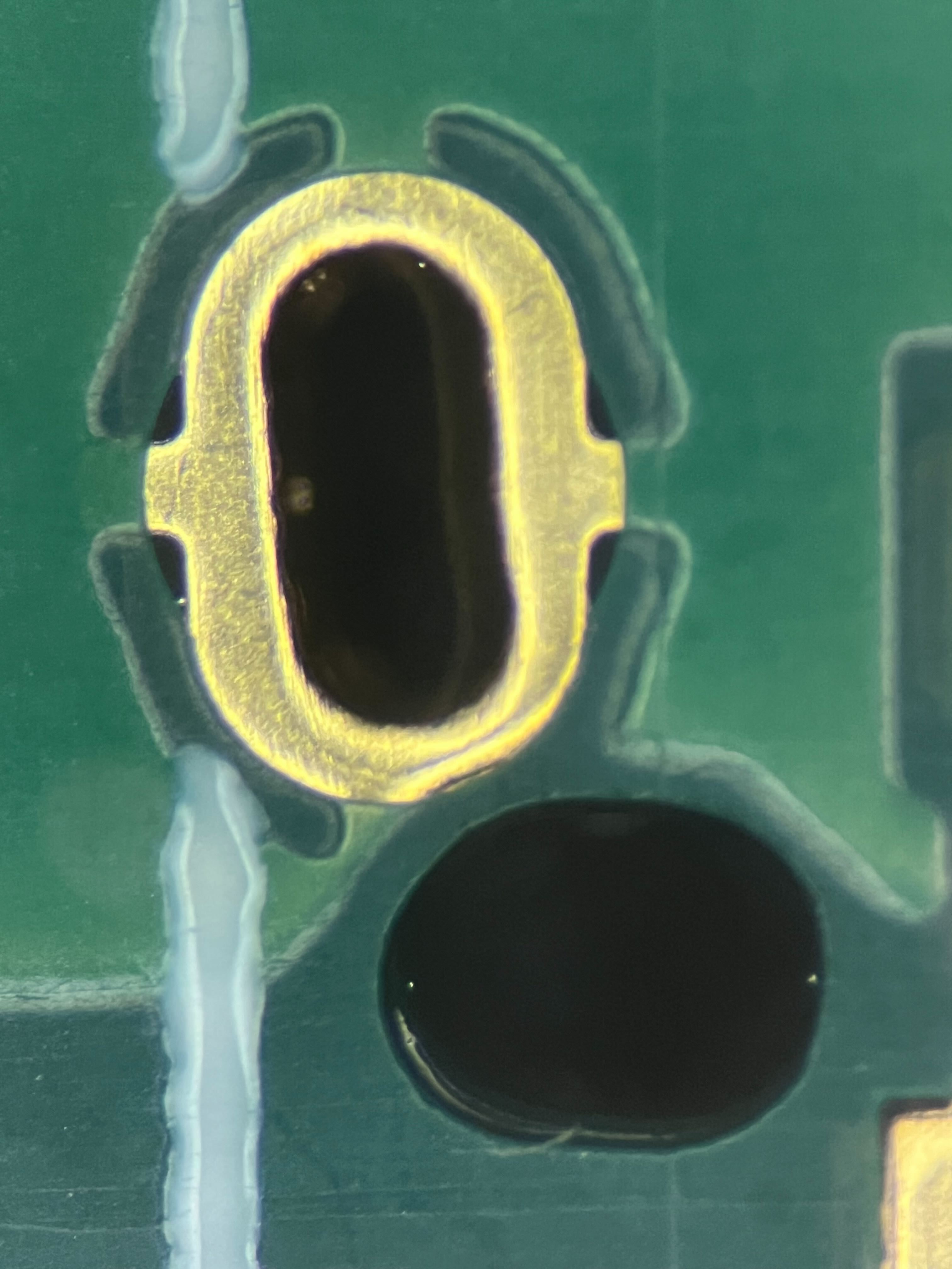 Figure 8: Manufactured board features