Eagle Layer Setups
How to define a 2 or 4 layer PCB
 Eagle allows users to define a number of different stackup configurations in the board editor DRC settings. Currently FlashPCB does not support blind or buried vias for our online quoting process. If you need these please email us at hello@flashpcb.com and we can quote them for you manually.
To change the number of layers in eagle go to the DRC editor under tools DRC and then open the layers tab.

Board Layer Count Errors
In our online quoting process, we are looking for either 2 or 4 layer boards without blind or buried vias. Our design rule check to see that the setup is either “(116)” for two layers to “(1+215+16)” for four layers. If you need more layers or blind or buried vias please email us at hello@flashpcb.com and we can quote them for you manually.
Changing Layers
To add layers to your board you can either use the drop down menu or the plus button.
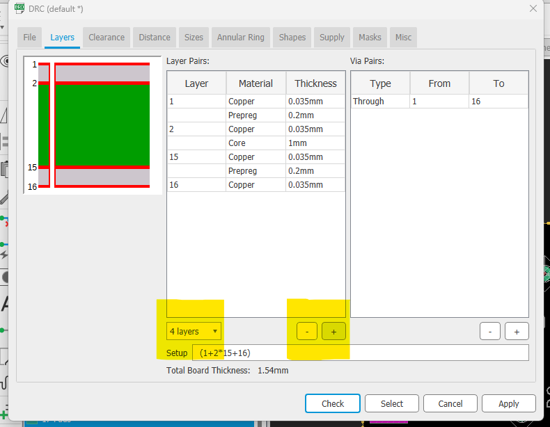
As the number of layers changes you will see the setup value change from “(116)” for two layers to “(1+215+16)” for four layers. This value indicates the layers and the substrates between them. The “*” indicated a core layer between the copper layers and the “+” indicated a prepreg layer between the copper layers. So in our four layer example there is a core substrate between the two inner layers, this is a 39mil FR-4 core in our standard four layer stackup, and a prepreg layer between the top copper layer and the inner layers and the bottom copper layer and the inner layers.
The stackup thicknesses in Eagle are not used in our manufacturing process they are subsituted for our standard 2 and 4 layer stackups.
Changing Via Pairs
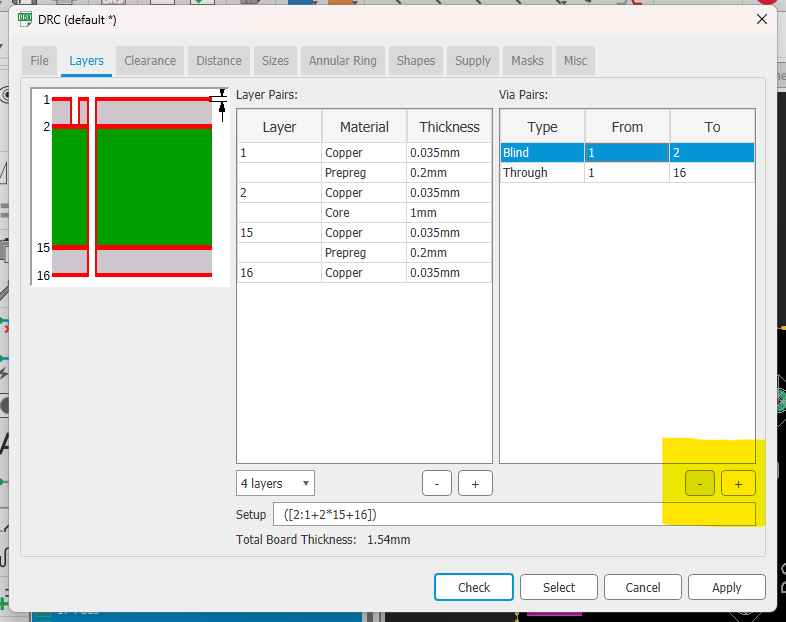
As via pairs are added you will see the setup value change. The through or buried vias are indicated with a set of parentheses, “()”, between the layers the via pairs. So in the standard four layer value of “(1+2*15+16)” there is a though via through all the layers.
Buried vias are vias that only connect inner layers of the pcb and not the top and bottom copper layers. If a buried via pair was added between the two inner layer then a the “215” layers would get an extra parentheses and become “(1+(215)+16)”, this would then fail our online design rule checks.
Blind vias are vias that connect either the top or bottom layer of copper to the inner layers of the board but not the other corresponding outer layer. Blind vias are indicated by a set of square brackets, “[]”, and a colon, “:”. The colon shows the layers the blind via will go to while the square bracket indicated the presence of the blind via. So for instance if a blind via was added to our standard four layer board connecting the top layer of copper to the top inner layer of copper, layers 1 and 2, we would add square brackets indicating a blind via and “2:” prior to defining the layers indicating the blind via would go though layer 2. This would then become “([2:1+2*15+16])” and would fail our online design rule checks.
Manufacturing Complex Boards
If you have any question or need more layers or blind or buried vias please email us at hello@flashpcb.com and we can quote them for you manually.